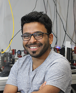
Stephen Edward
PhD student in the Light-Matter Interaction group
Ultrasound Isn’t Just for Babies. It Could Also Help Build a Better Computer Chip.

However, in an actual industrial scenario, the all-important markers get buried under multiple opaque layers, making it difficult for the machines to find them using light and align for the printing process.
“The machines need to be able to see through the opaque layers to find the markers. It’s like building a skyscraper. You need to know where the first floor is when you build the tenth floor,” says Stephen Edward, a metrology PhD student in the group of Prof. dr. Paul Planken at ARCNL, the Advanced Research Center for Nanolithography. Stephen and his group’s solution is to use a high-powered laser. The laser launches extremely high-frequency soundwaves (ultrasound) into the layers and reads out the echo. Ultrasound can travel through layers that light can’t, allowing machines to look through the usually-opaque layers and find the markers. “It’s a bit like knocking on a wall to figure out if there’s a hard object or empty space behind it. The only difference here is that instead of knocking on the wafer, we use laser light to create the sound and “listen” to it using laser light,” explains Stephen.
If using light to create ultrasound sounds a little science fiction-y to you, you’re not alone. “When I joined four years ago and my supervisor told me this was the project, I thought the idea sounded impossible. You hit an object with light and it becomes sound! I didn’t know that was even possible,” Stephen says. At some point, it started to seem less far-fetched though, and one year ago the group was able to show for the first time that it was possible to use sound waves to detect markers hidden under metal and dielectric layers.
Now that this technique has been shown to work in a lab setting, the next question is how quickly it could be transferred to an industrial setting. ARCNL is a public-private partnership between two universities in Amsterdam (University of Amsterdam and Vrije University Amsterdam), the Dutch Research Council (NWO) and ASML, a Dutch company that is the world leader in the production of machines that make processors and memory chips for computers, tablets, and smartphones. The institute’s close connection to industry is what attracted Stephen to ARCNL in the first place. “I liked the idea of doing something that would allow me to jump into industry quickly,” he says. “I didn’t want to work on something that was really abstract and wouldn’t have any practical applications at all in the next 50 years. That’s the highlight of this institute I would say, that you get to work directly with industry.”
Another highlight for Stephen is the community feel of ARCNL. The institute has 75 employees in total which means you quickly get to know everyone else who works there and feel comfortable approaching other professors and group leaders. The fact that everyone works on interrelated projects adds to the community feeling. “When I hear from other international students, one of the complaints I hear is that they feel isolated in a new country and they don’t get to mingle with the local crowd. That’s not the case here. My friends are mostly from work which is great,” he adds.
Extreme ultraviolet lithography, Stephen’s research area, is the most promising new technology for computer chipmaking. By combining fundamental physics with inspiration from industry, he and his ARCNL colleagues are pushing boundaries and contributing to the development of smaller and smarter electronics.
‘This article was first published on www.academicstories.com‘


