Group leader: Dr. Lyuba Amitonova
Nanoscale Imaging and Metrology
Research activities Nanoscale Imaging and Metrology
Machine Learning for Imaging and Metrology in the Semiconductors
The ever-increasing computational power and ever-shrinking size of electronic devices have been enabled by rapid developments in optical lithography and the micro-electronics industry. State-of-the-art processors require reliable and fast nanoscale engineering methods with high production efficiency. The widespread access to computational power has already made a big impact on our daily lives. New future applications like VR, AR or AI technologies require even smaller and more powerful hardware. However, keeping up with the aggressive reduction of the semiconductor device feature sizes is a challenging task.
In this project, we will explore deep learning and Bayesian optimization techniques to push the boundaries of compact semiconductor metrology tools. Label-free optical imaging methods with a spatial resolution beyond the Abbe diffraction limit and a temporal resolution beyond the Nyquist limit are being developed to characterize multi-layer nanostructures. Several modern research areas such as computational imaging and compressive sensing are connected with cutting-edge Machine Learning tools to develop new methods of nanoscale imaging and metrology for the semiconductor industry. The project is running in collaboration with the AI4Science Lab at the University of Amsterdam and ASML, the world leader in the production of the lithography machines.
Computational fiber imaging
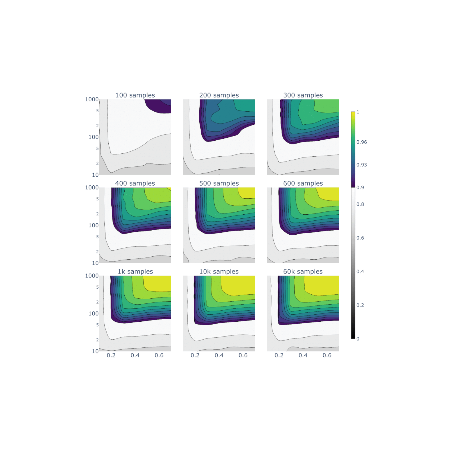
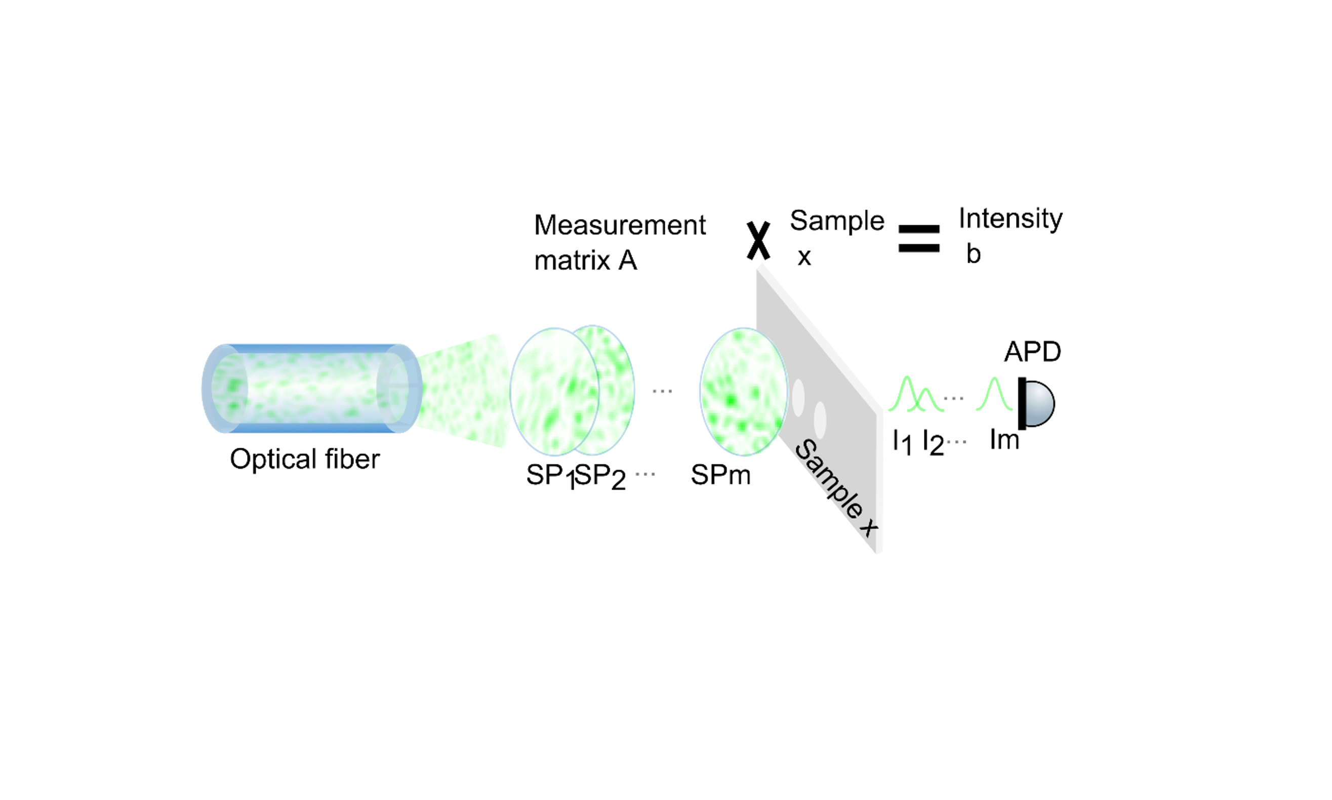
Optical fibers, with their compact and flexible nature, are ideal imaging tools across diverse applications ranging from nanolithography to biomedical sciences. Conventional imaging systems face limitations in spatial resolution and imaging speed due to Abbe and Nyquist constraints. Computational imaging is an innovative concept that explores the idea of joint optimization of optical hardware design and signal post-processing algorithms to transcend these boundaries. In terms of hardware, we design different fibers and investigate the parameters for the best performance on numerical aperture, losses, and signal-to-noise ratio. On the software side, advanced compressive sensing algorithms capitalize on the inherent sparsity of samples and the uncorrelated nature of speckles in optical fibers. This allows us to reconstruct images that exceed the Abbe diffraction and Nyquist limits.
By Zhouping Lyu
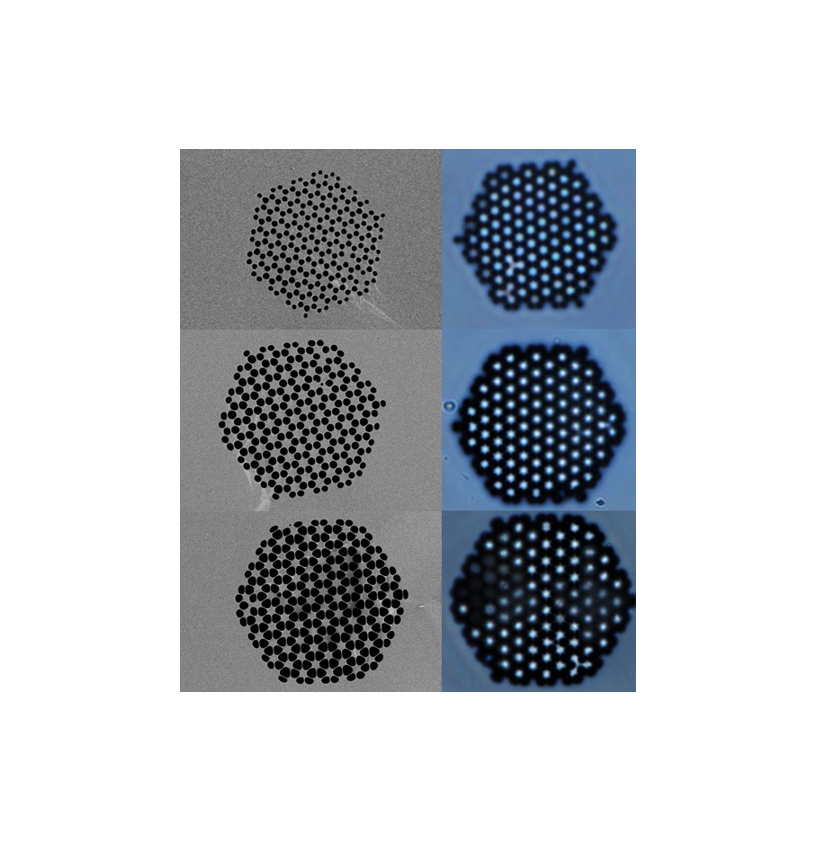
Multicore fiber sensing
The challenge of fabricating high performance microchips capable of sustaining the ever increasing demand of data storage and computing power is accompanied by increasing complexity in fabricating one with very high precision and accuracy. Inspecting if the microchips are properly in place during the fabrication procedure is where metrology comes into play. The most sophisticated microchips having structures of 10 nanometers in size, forces researchers to design novel methods and experiments to measure the quality and position of these structures, pushing the boundaries far beyond the limitations set by Abbe and Nyquist, present in more conventional methods.
Using theoretical calculations and extensive numerical simulations, multicore fiber sensing is a novel imaging method which continues to be explored theoretically by optimizing the multicore fiber design, and challenged experimentally to prove the concept. With theory and experiment in a harmonious balance is multicore fiber sensing pushed to its maximum potential in order to achieve the goal of sensing the smallest targets with the highest accuracy and precision. This project is one of the most collaborative projects so far, collaborating with the Free University of Amsterdam, University of Twente, Max-Planck-Institut and ASML.
By Kian Goeloe

Coherence control via multimode fiber for optical metrology
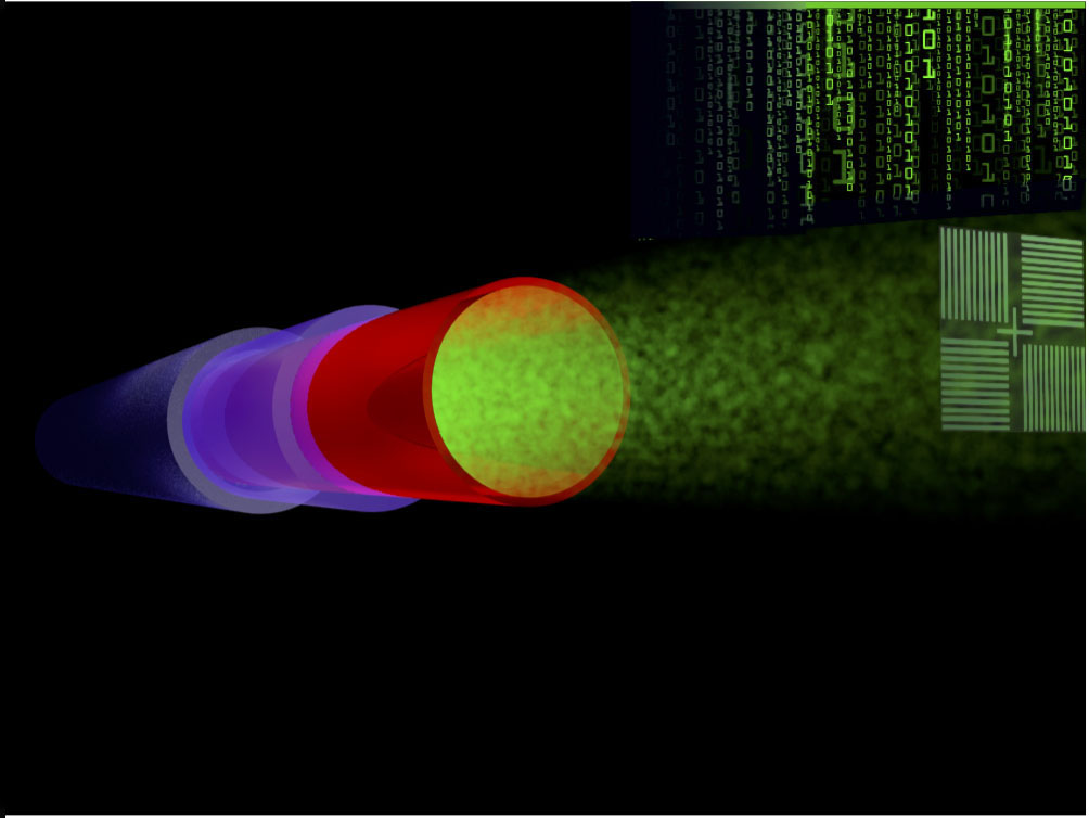
Coherence is a key aspect of light, playing a crucial role in enhancing the precision of light sources used in ASML metrology applications. Our research focuses on the development and investigation of an innovative, cost-effective instrument designed to tune the spatial coherence of a bright laser source. The use of a simple multimode fiber, as depicted in the following figure, looks as a highly promising approach for controling spatial coherence. Multimode fibers are capable of supporting thousands of guided modes, offering a broad array of options to optimize various light properties, including spatial coherence.
Achieving complete control over the coherence and wavefront through a compact, low-cost fiber-based system could notably improve both accuracy and reliability in semiconductor metrology.


