Pulsed Laser Deposition for Materials and Surface Science
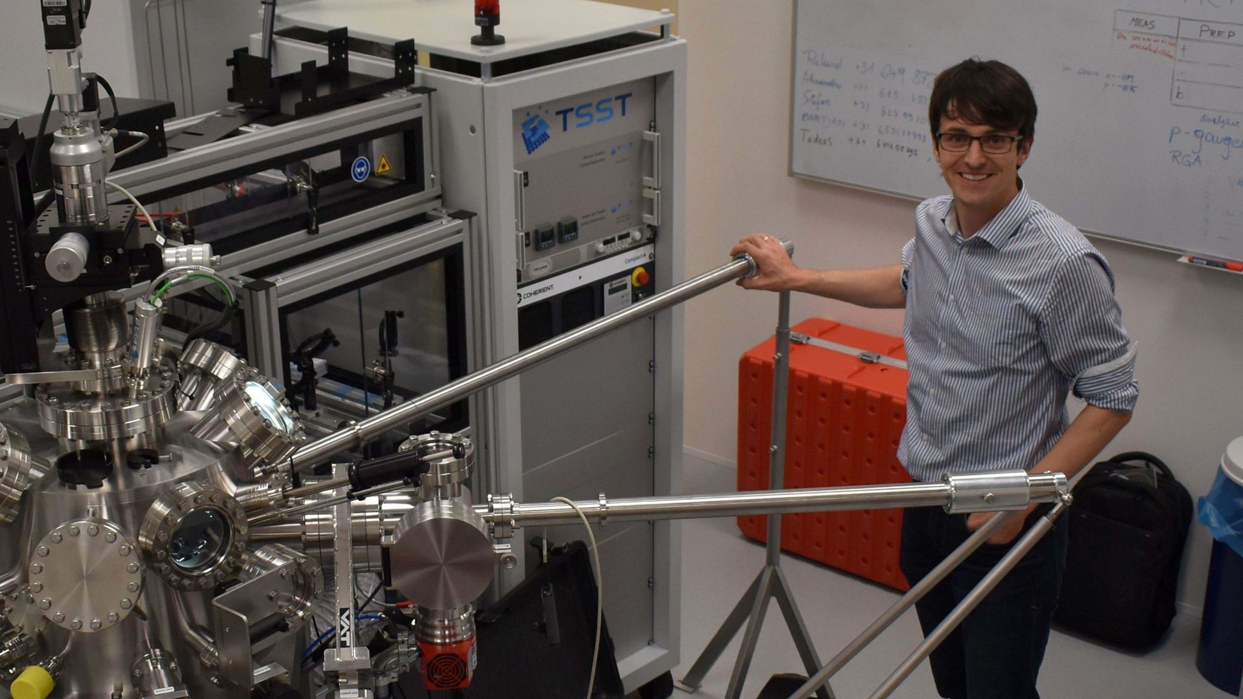
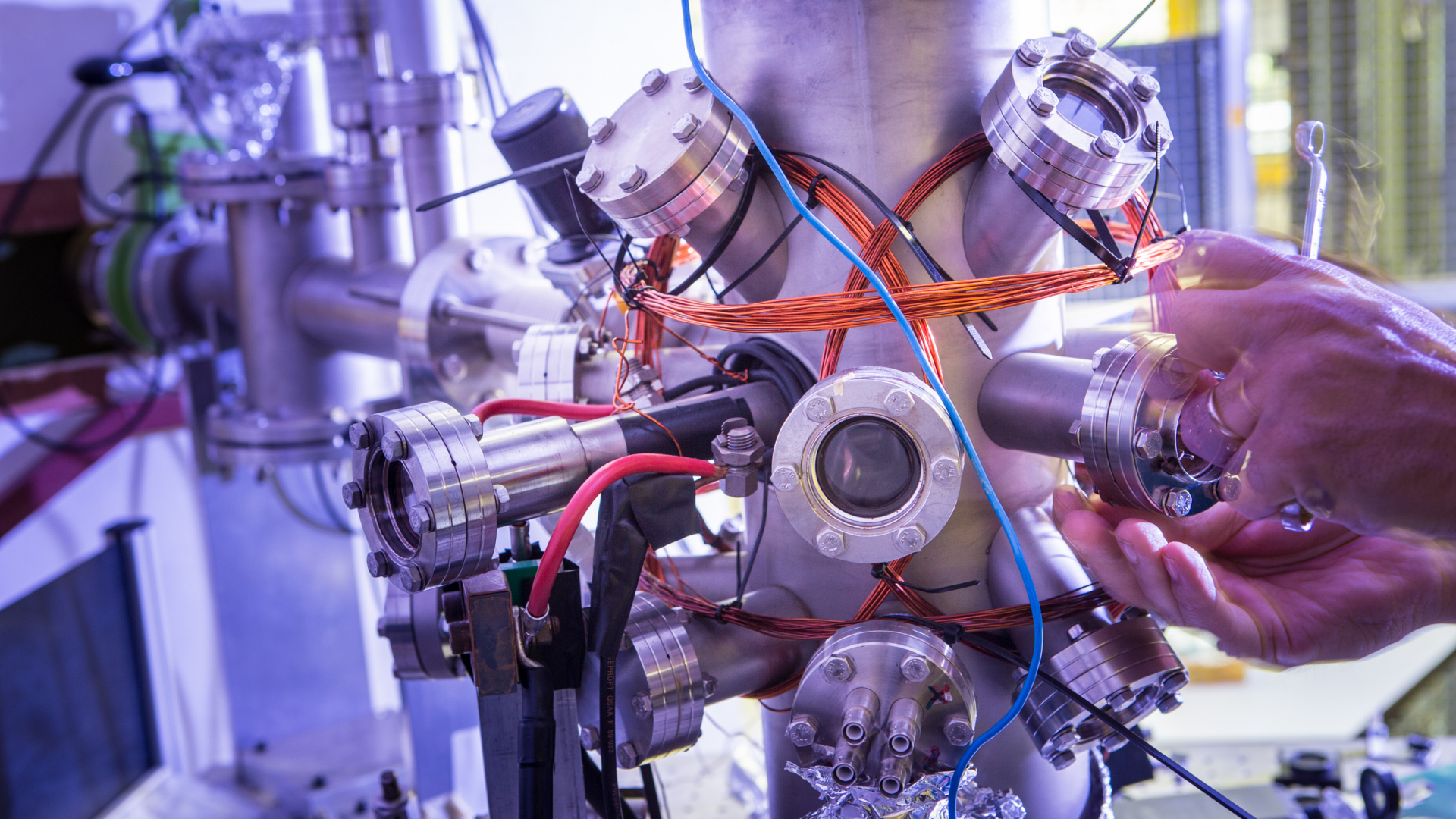
In the lab for Materials and Surface Science for EUV Lithography the long awaited setup for thin-film growth using pulsed laser deposition (PLD) has recently been installed. The new setup is fully integrated with the group’s X-ray photoelectron spectroscopy (XPS) device for growth, transfer, and analysis in ultra-clean conditions. Right after growing a film using PLD, it can be transferred to the XPS chamber without leaving the ultra-high vacuum environment, thus providing an ideal starting point for studying sample composition, surface chemistry, and reactivity close to the conditions used in nanolithography setups or in catalysis.
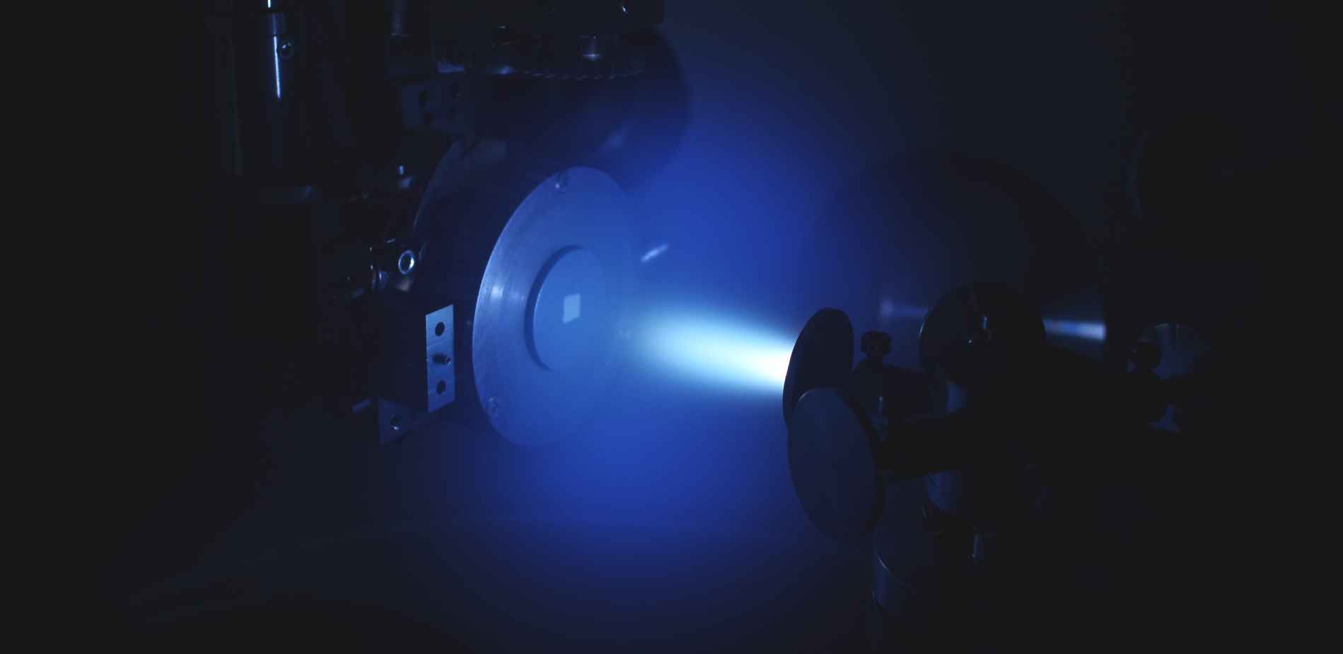
Pulsed laser deposition is one of the most versatile methods for thin-film growth. Inside an ultra-high vacuum chamber the material of interest is hit by high-intensity laser pulses. At every pulse material is “ablated”, meaning that the laser pulse supplies enough energy to the target material to locally create a plasma of identical composition. This material expands away from the interaction region into the vacuum chamber, where it can be collected and grown as thin film on a substrate. This process is often used to grow complex oxides and ceramics, but it can produce thin films of almost any solid at the composition of choice. By changing the properties of the laser pulses, the substrate material, and the atmosphere in the chamber we can explore different structures of thin films of the same material: from single crystalline to amorphous.
Pulsed laser deposition will play a central role in the Materials and Surface Science group’s core research on amorphous materials and their surface chemistry. Group leader Roland Bliem says he is excited about the new capabilities introduced by PLD and his group plans to make use of its full potential for the growth of materials ranging from metals to semiconductors and ceramics.