New perspectives on light-induced damage
ARCNL alumnus Ester Abram conducted her PhD research on how high-intensity laser light can damage material surfaces, with an interest in semiconductor manufacturing processes. Now, she and her collaborators from ARCNL and ASML have expanded on this work in an extensive Perspective study, now published in the Journal of Applied Physics. In it, the team shares a vision of future challenges and possibilities for using light-induced damage, for example as a tool in fabrication and sensing.
An exciting request
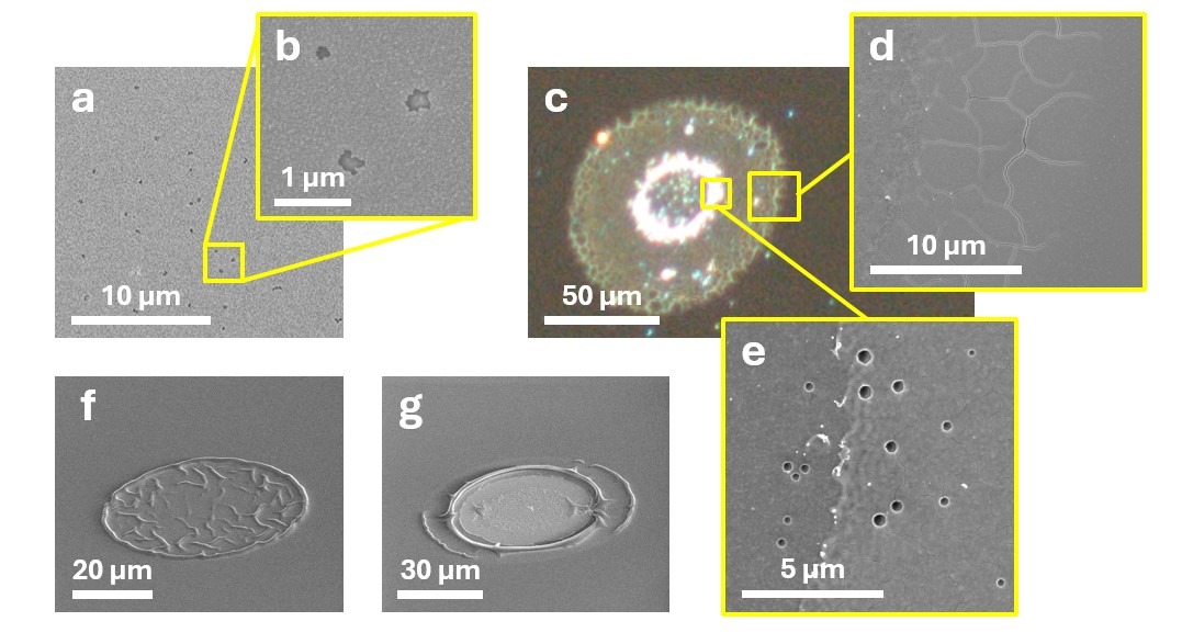
During her PhD at ARCNL, VU Amsterdam postdoctoral researcher Ester Abram focused on one of the central challenges in computer chip manufacturing: what happens when intense laser light interacts with materials at very small scales. In semiconductor fabrication and inspection, laser light could cause damage to materials if the intensity is too high. But what Ester found was promising: at relatively low light intensities, small changes to the material can already be seen before catastrophic damage occurs. This implies that these changes can also serve as warning signs, making it possible to prevent irreversible damage during intermediate inspection stages.
Ester’s findings proved to be of high interest to the broader research community, and she and her collaborators were invited by the Journal of Applied Physics to write a so-called Perspective paper on light-induced damage within the context of semiconductor device manufacturing. Ester and her co-authors Reynolds Dziobek-Garett, Roland Bliem and Paul Planken of ARCNL and Vina Faramarzi of ASML, brought together knowledge from different research directions, materials, and light sources. The result is an overview of current challenges, as well as emerging opportunities, for anyone working with light in chip fabrication and optical inspection.
Writing a Perspective paper presents a different kind of challenge than other research papers, as it comprises both a review of research in the field and the authors’ own visions for future developments. “We feel honored to be asked to write this paper,” shares Paul, principal investigator for the project. “The challenge is: how does one select which topics to cover, and how can we do justice to all the research that has been done in the world in this field?”
The diverse backgrounds and perspectives among the authors were helpful in creating a broad overview. “With the help of Vina, who works at ASML, we got input about all sorts of light sources that could be used,” shares Ester. “Reynolds works with a new type of material, 2D materials, which will be very relevant in the future. Meanwhile, Roland provided more information from a chemical perspective.”
New opportunities for nanoscale processes
The key message is that in the semiconductor device manufacturing industry, new materials and light sources will lead to new challenges, but also to new opportunities. Under controlled conditions, for example, light can be employed to modify materials, fabricate structures, or even enable new sensing methods. “We realized there are many more possibilities to use light-induced damage in a beneficial way,” Ester explains.
By mapping out where damage occurs, why it happens, and how it might be controlled, the authors aim to support the development of next-generation fabrication and inspection techniques. As chip components continue to shrink and new materials are introduced, understanding these light-matter interactions becomes increasingly important.
Now published in the Journal of Applied Physics, the Perspective paper can be read as an agenda for the field, highlighting where fundamental understanding is still lacking and where new approaches could push the limits of what is currently possible in semiconductor manufacturing. For researchers and engineers working on future chip technologies, it offers both a summary of what is known and a guide to the challenges that lie ahead.
Contact
For more information about this work, contact Paul Planken (email: P.Planken@arcnl.nl).
Publication
Ester Abram, Reynolds Dziobek-Garett, Vina Faramarzi, Roland Bliem and Paul Planken, Light-induced damage in semiconductor device manufacturing: Present and future challenges, Journal of Applied Physics 139, 080901 (2026). DOI: 10.1063/5.0308054


