New Paper! Nanometer interlaced displacement metrology using diffractive Pancharatnam-Berry and detour phase metasurfaces
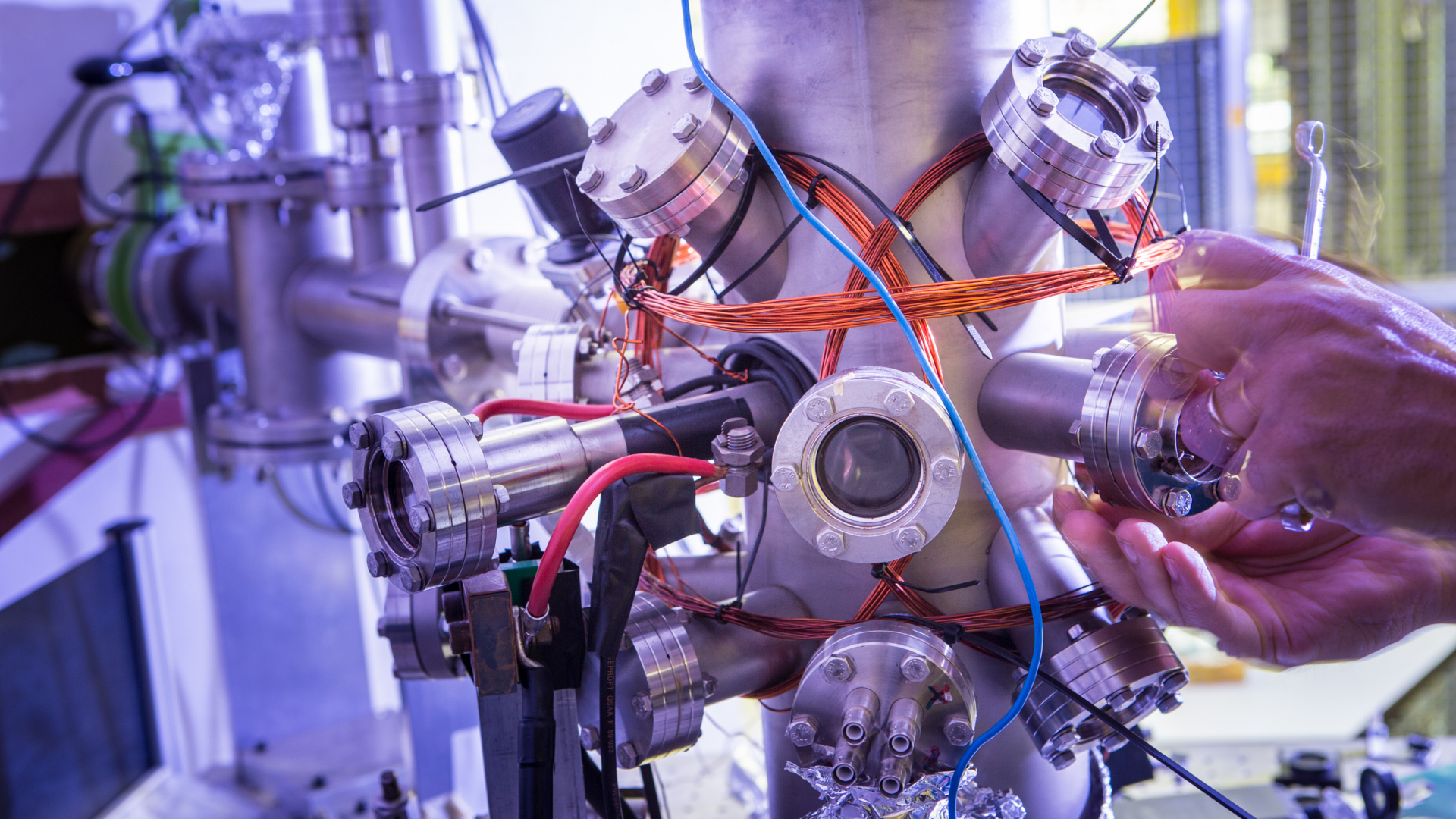
We are excited to announce the publication of our latest research, a collaborative effort between the Resonant Nanophotonics group at AMOLF and the Nanoscale Imaging and Metrology group at ARCNL. This groundbreaking study presents a novel method for measuring sub-nanometer displacements between periodic nanostructures—a significant advancement in the field of metrology [1]. As the semiconductor industry continues to innovate to produce microchips with high computational power, assessing the quality of a microchip becomes challenging. State-of-the-art microchips contain nanostructures approximately 10 nm in size. Careful alignment of these nanostructures is vital for optimal performance of a microchip. This is done utilizing diffraction gratings and measuring the intensity difference between the diffracting orders, which is related to the alignment of the nanostructures on the wafer. The method proposed in [1] distinguishes itself utilizing measuring the full polarization state of the diffracted signal, rather than intensity only.
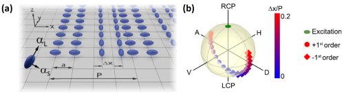
The concept is demonstrated using a metasurface, which consists of a 2D array of highly refractive nanostructures (meta-atoms) and can be used to alter fundamental properties of the incident electromagnetic wave [1]. The meta-atoms on the metasurface have a distinct polarizability along the long- and short-axis, denoted αL and αS, respectively (Fig. 1a), and are periodically structured by alternating the orientation of each pair of meta-atoms with 90°, ultimately creating a diffraction grating. Following the concept of the Pancharatnam-Berry phase, by exciting the diffraction orders with circular polarized light, the resulting diffraction orders obtain the opposing circular polarization with respect to the incident polarization. However, if a pair of meta-atoms are displaced by Δ𝑥 within the diffraction grating, the resulting polarization of the +1st and -1st diffraction obtain marked elliptical polarization as highlighted on the Poincaré sphere in Fig. 1b, which is a result of so-called detour phase shifts induced by the displacement. The unique combination of the Pancharatnam – Berry and detour phase shifts thus transduces deeply subwavelength displacements within a device layer into specific polarization signatures in the diffraction orders of the metasurface. This novel method has the potential to revolutionize the semiconductor industry with more accurate alignment and can be tailored to displacement sensitivity in two dimensions. Additionally, given that this method uses polarization to extract alignment information makes it robust to noise, and allows for defining true zero, making any form calibration or use of a reference obsolete.
References:
[1] Feldman, Nick, et al. “Nanometer Interlaced Displacement Metrology Using Diffractive Pancharatnam-Berryand Detour Phase Metasurfaces.” ACS photonics 11.12 (2024): 5229-5238


