Inspecting moving surfaces with a lensless microscope
ARCNL, VU University Amsterdam, ASML and Tata Steel collaborate in an STW project.
Researchers from ARCNL, VU University Amsterdam, ASML and Tata Steel are joining forces to develop new techniques for imaging surfaces based on lensless microscopy. They are working together in a project funded by Technology Foundation STW that starts on 1 December 2015. The project has a duration of four years and a budget of 700,000 euros. ASML and Tata Steel are contributing 15% of the total amount each.
The project fits within ARCNL’s objective of acquiring fundamental knowledge that could form the foundation for possible applications. ARCNL’s research is always curiosity driven, but with high-tech applications in mind. Project leader Stefan Witte: ‘ARCNL is developing knowledge on lensless microscopy. This knowledge is not only proving relevant for the lithographic structures that ASML uses, but also for Tata Steel’s rapidly moving metal surfaces.’ This means that, after ASML, Tata Steel is the second company that ARCNL will be collaborating with.
Lensless microscopy
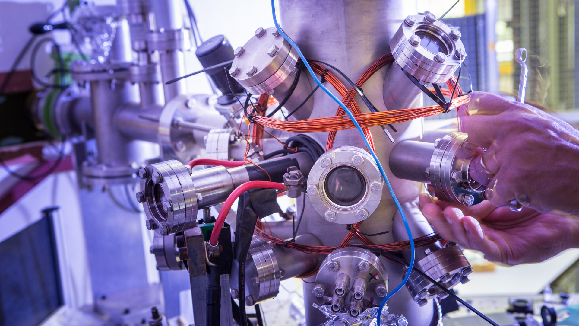
The aim of the project is to develop new microscopes to be able to examine both rapidly moving metal surfaces and lithographic structures during production processes. Witte: ‘For industrial applications, the structure of the surfaces must be exactly right and free of defects. We therefore want to be able to examine the surfaces with microscopes even during the production process. Lensless microscopy is an imaging technique in which the image of an object is not directly projected with lenses. Instead, a camera records light scattered by the object. The result is often an unrecognisable image that nevertheless contains a lot of information about the object. However, with the help of computer software, we can still reconstruct the shape of the object examined. Using this approach, we can build more compact and flexible microscopes that can nevertheless provide very sharp images.’
High Tech Systems and Materials
The project has been awarded funding within the High Tech Systems and Materials (HTSM) call, which is organised annually by STW with a contribution from Stichting TKI-HTSM. HTSM is one of the nine top sectors identified by the Dutch government and is therefore a direct outcome of government policy. The HTSM Call is open for projects in which researchers enter intensive collaborations with companies to develop fundamental knowledge for technological breakthroughs and innovative applications.
About ARCNL
The Advanced Research Center for Nanolithography (ARCNL) is a public-private partnership between the Foundation for Fundamental Research on Matter (FOM), the University of Amsterdam (UvA), VU University Amsterdam (VU) and the semiconductor equipment manufacturer ASML, with additional financial support from Amsterdam City Council and the Province of North Holland. ARCNL focuses on the fundamental physics involved in current and future key technologies in nanolithography, primarily for the semiconductor industry. A significant part of the initial program is devoted to the physics that is central in the generation of high intensities of extreme ultraviolet (EUV) light and its use in nanolithography. ARCNL is located on the Amsterdam Science Park.An ‘Advanced Research Center’ is a new type of partnership with which NWO wants to provide a boost to collaborations between universities and private parties.