HTSM funding for Paul Planken and Stefan Witte
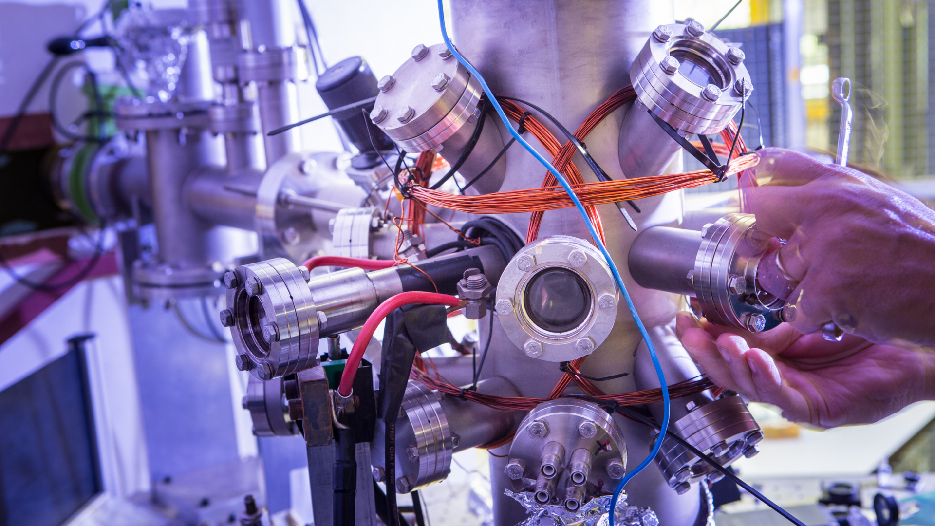
ARCNL group leaders Paul Planken (also full professor at the Institute of Physics at the University of Amsterdam) and Stefan Witte (also associate professor at the department of physics at the VU Amsterdam) both have been granted a project within the program High Tech Systems and Materials (HTSM) of NWO. Stefan Witte’s project ORPHEUS is in collaborations with VU and ASML. In the Wafer damage control project Paul Planken collaborates with Dries van Oosten of the Debye Institute for NanoMaterials Science (Utrecht University) and the companies ASML and ALSI.
About the projects
ORPHEUS: Opaque and Reflective nanostructure Probing using Hypersound Excitation with Ultrafast Sources
The ability to look through opaque materials is an intriguing concept, with many potential applications in science and technology. While a layer of opaque material by definition does not transmit light, in various cases other types of waves can penetrate through it. One example of such a wave is ultrasound, which is well-known and used in biomedical applications for e.g. looking inside tissue. In this project, researchers from VU, ARCNL and ASML join forces to investigate the potential of laser-induced ultrasound for probing structures below opaque layers. Ultrafast lasers can produce extremely short ultrasound pulses inside an opaque material, which can in turn be used to probe buried structures underneath this layer, and possibly even retrieve full 3D structural information and material properties of hidden features. The potential of this concept for the detection of nanostructures will be explored, which may enable innovative new metrology techniques for the semiconductor industry.
Wafer damage control: understanding and preventing light-induced material changes in optical measurement systems
In the semiconductor industry, advanced optical sensors are used throughout the lithographic process. They play a vital role in nanolithography and help to keep Moore’s law going. These sensors use more and more powerful light sources to increase signal strength, increasing the risk of optical damage. In collaboration with ASML, the research described in this proposal aims to classify the different kinds of optical damage and, more importantly, to understand the fundamental mechanisms responsible for the damage. In many cases little is known about the damage thresholds and damage mechanisms in industrially-relevant materials such as amorphous carbon or Si3N4. With the knowledge that we acquire in our research we will be able to develop numerical models that can predict when damage occurs and how to reduce the risk of damage.
About HTSM
The High Tech Systems and Materials (HTSM) program challenges researchers and companies to jointly develop knowledge for technological breakthroughs and innovative applications. The annual call for proposals of HTSM, organized by NWO Domain Applied and Engineering Sciences (AES), is a consequence of the top sector policy initiated by the Dutch government. This year a total of 22 projects can start.
Read the news release on the NWO website


