
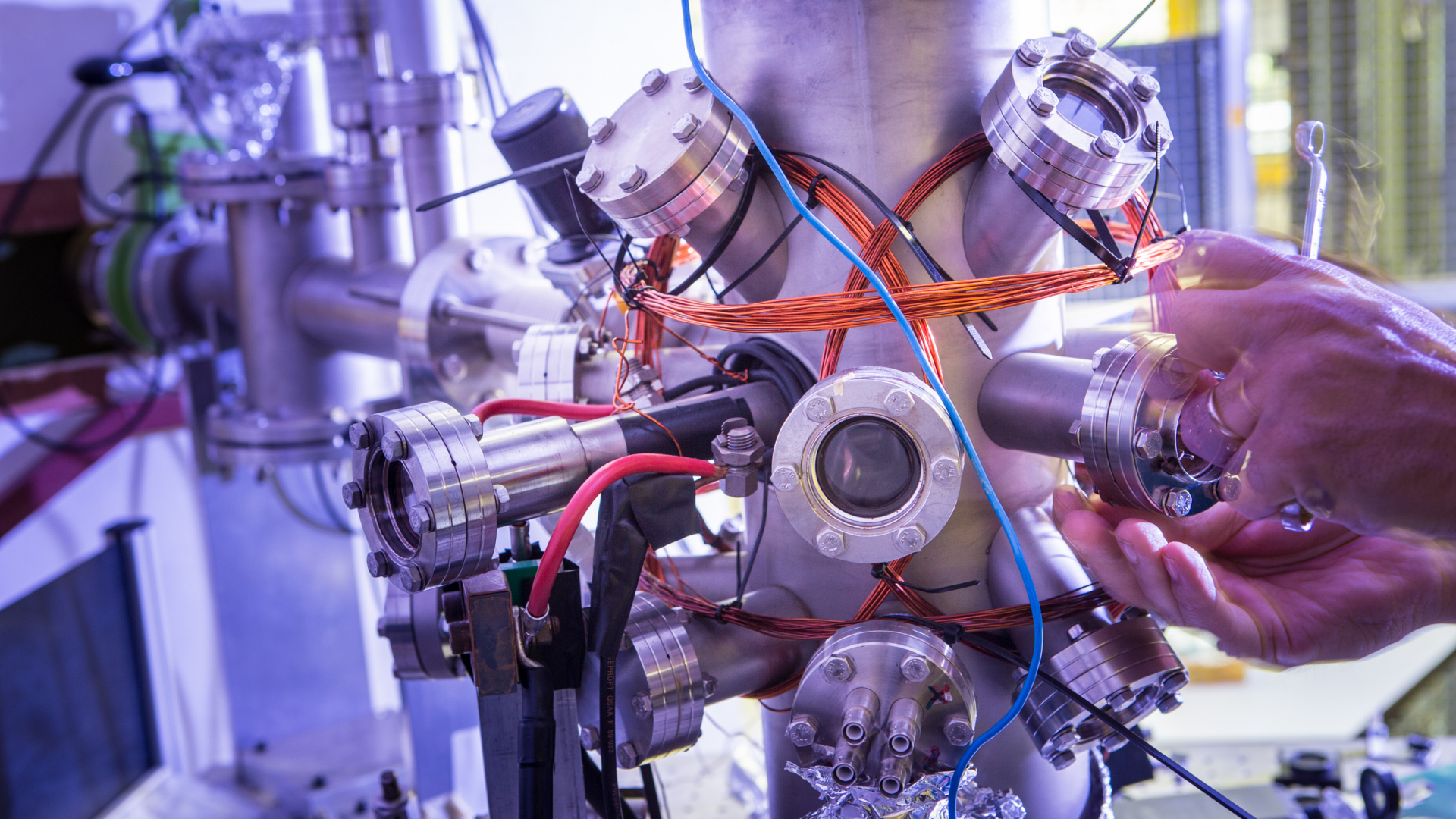
Unique collaboration demonstrates promising new imaging tool
Two-dimensional semiconductor films, which can be only atoms thick, are promising materials for next-generation electronic devices. However, challenges with measuring defects in the films have made them difficult to implement industrially. To tackle this challenge, academic and industry researchers came together to develop an imaging technique using second harmonic generation, laying the groundwork for implementation in semiconductor device manufacturing.
Industry-inspired experiments
In the pursuit of smaller, more powerful, and more energy-efficient computer chips, researchers are exploring the potential of 2D semiconductor films. These materials are called “2D” because they can be as thin as a single layer of atoms, which also gives them unique electrical and optical properties.
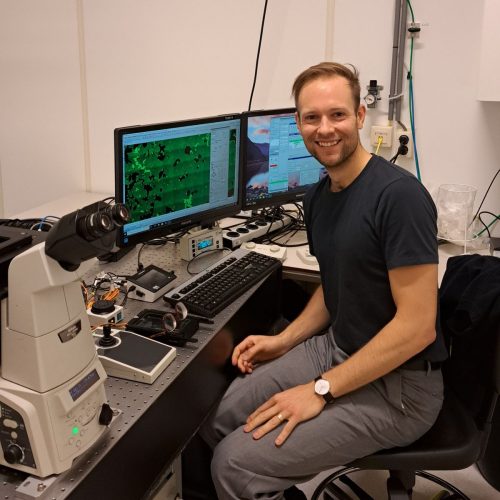
However, those same unique properties also make them more difficult to image using commonly used techniques. This is especially challenging at the scale of the silicon wafers used in fabrication, which are around 30 centimeters in diameter. This challenge inspired ASML researchers Dr. Vina Faramarzi and Dr. Vasco Tenner to reach out to ARCNL postdoctoral researcher Dr. Reynolds Dziobek-Garrett, whose work focuses on such 2D materials.
They asked whether they could develop a measurement technique based on second harmonic generation (SHG), which has proven useful in materials science and some medical applications. Dziobek-Garrett was excited to collaborate with them: “Working with industrial partners to convert ideas into experiments and then convert the results back into industrial relevance is something that motivates me.”
Collaborative detective work
In order to properly demonstrate any technique’s usefulness for semiconductor fabrication, the team needed access to samples of state-of-the-art materials relevant to industrial applications. This was possible via imec-ASML long-standing strategic partnership agreement.
“Through the strategic partnership framework, we had access to industry-grade 2D molybdenum disulfide (MoS2) films grown at imec by Dr. Pawan Kumar as part of imec’s exploratory logic R&D program. We could make these films available to our research partners in ARCNL,” explains Faramarzi. “Subsequently, ARCNL was formally included as a partner in our existing project with imec on 2D materials.”
The idea was that, because a stack of two of these films has nonlinear optical properties, the stack could be used as a medium for SHG, also known as frequency doubling. In this process, light interacts with the material such that the light that comes out has double its original frequency. By looking at where in the sample this happens, you can deduce the arrangement of atoms in the stack, and thus the alignment of the two thin layers.
Imaging using SHG proved to be useful in combination with other imaging techniques. “This project required a bit of detective work,” says Dziobek-Garrett. “Each imaging technique we used gave different information about the sample. So only by comparing the images can we see the complete picture of the films we analyze.”
A new, scalable technique
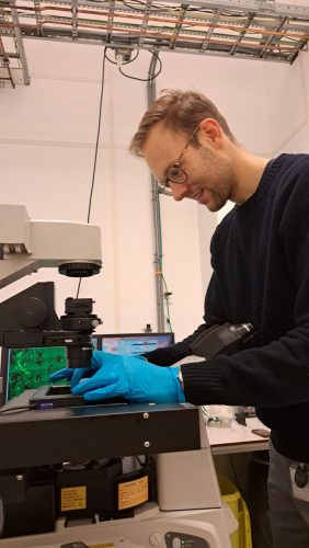
Dziobek-Garrett and his collaborators demonstrate their new technique in a new publication in the journal Applied Physics Letters. “We discovered that SHG is a useful technique for measuring 2D semiconductor films,” he says, “and that it can provide unique information about the sample compared to commonly used techniques.”
This work is an example of the impact that strong industry-academia collaborations can have. Developing next-generation technologies often requires expertise, infrastructure, and materials from multiple organizations, and partnership frameworks such as those between ASML, ARCNL, and imec play an important role in enabling these advances.
What is especially exciting about this finding is that it can be further developed into a full-wafer analysis tool. “Using samples that were grown in an industry-relevant way, we were able to demonstrate the technique for rapid, large-area analysis of bilayer stack alignment,” says Dziobek-Garrett. “This makes it promising for future implementation in the semiconductor industry.”
Contact
For more information about this research, please contact Dr. Reynolds Dziobek-Garrett (R.DziobekGarrett@arcnl.nl).
Publication
Reynolds Dziobek-Garrett, Vina Faramarzi, Pawan Kumar, Vasco Tenner, Marko Kamp, Femius Koenderink, Jorik van de Groep, & Roland Bliem. Rapidly resolving bilayer stacking orientation in industrially compatible MOCVD-grown MoS2 films through second harmonic generation imaging. Applied Physics Letters 129, 092105 (2026). DOI: 10.1063/5.0334162


