Detecting hidden nanostructures by converting light into sound
Researchers at ARCNL have found a way to detect nanostructures buried under many layers of opaque material, using very high frequency sound waves induced by light. Their findings are promising in view of applications in the semiconductor manufacturing industry, such as wafer alignment. The researchers also revealed interesting new phenomena in photo-acoustics that have not been investigated before. They publised their results in Physical Review Applied on 7 July. First author of the article, Stephen Edward successfully defended his PhD on this subject on 18 June at the University of Amsterdam.
In the production of state-of-the art computer chips and components, nanolithography machines print several layers of nano-size structures on a wafer. To make sure the layers are aligned accurately, wafers contain grating lines that act as markers that tell the machines where to print. “While alignment markers are indispensable in nanolithography, they get buried under many layers of material. Because these layers are often opaque, it is difficult to use light to find the markers and align the machine”, says Stephen Edward, who carried out his PhD research in the Light-Matter Interaction group at ARCNL.
‘Seeing’ with sound
Many materials that are opaque (i.e. not transparent) for light, do transmit sound waves, that can also be used to visualize what is underneath. Group leader Paul Planken: “Most people are familiar with this in a medical situation. Echoscopes use high frequency sound waves that are reflected inside the body at the interface of different tissues. The reflected sound waves are converted to an electric signal to create an image. While this method contains enough detail for most medical applications, it is by far not detailed enough for accurate alignment in nanolithography. The size of the features that can be discerned with echoscopic methods is inversely proportional to the frequency. So, to be able to ‘see’ nanosize structures with sound, we need sound waves with a much higher frequency.”
‘Knocking’ with light
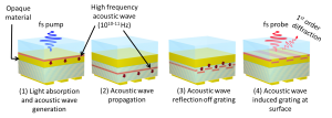
Planken, Edward and co-authors knew that short light pulses from a laser can induce such high-frequency sound waves in an opaque material. “It is a bit like knocking on a door, which causes sound waves to travel on to the other side of the door”, says Edward. “In our experiment, a high energy ‘knock’ of the laser starts a sound wave in the opaque material.”
Just like in medical applications, the sound waves traveling through the material are reflected off interfaces inside the material, causing a wave that travels back to the surface. When they first started, the researchers were not sure whether this signal would contain enough useful information. Planken: “I was a bit skeptical in the beginning, because the sound waves have to travel through so many layers of dielectric material before they reach the grating buried inside. If they reflect at all these interfaces, we would have ended up with a complete mess of sound waves. But it turned out that the stack of thin dielectric layers acts as one thick layer because the individual layers are thinner than the wavelength of the sound wave. So the sound waves travel straight to the buried grating lines that we want to see.”
‘Listening’ with light
The sound reflects at the grating. Since the grating is not a flat surface but has periodic valleys and peaks, sound from the valleys reaches the surface slightly later than sound from the peaks. “The sound wave causes a very small displacement of the atoms when it reaches the surface, causing a copy of the grating to appear at the surface”, Edward explains. “When we scan the surface with a second laser pulse, we can measure the diffraction signal caused by these small displacements.”
Now that they have shown that it is possible to detect nanostructures buried under opaque material, the researchers are going to further investigate their method. Planken: “Our results not only reveal interesting features in photo-acoustics that have not been investigated before, but also offer a promising solution for practical issues in nanolithography. For industrial applications, we should optimize the system to get signals that are stronger, faster and more robust. But we also want to increase our understanding of all the effects that we see in the signal, and find the limits of our method, for example by trying to discern a grating with lines that are very close to each other.”

A femtosecond pump laser ‘knocks’ at the opaque material (1), causing a high frequency acoustic wave to travel through the layers (2) until it reaches the buried grating lines. The acoustic waves are reflected at the grating and travel back (3) as a grating shaped wave. When this wave hits the surface (4), the grating shaped deformation can be detected from the diffraction signal of a femtosecond probe laser.
Reference
S. Edward, H. Zhang, I. Setija, V. Verrina, A. Antoncecchi, S. Witte, P.C.M. Planken, Detection of hidden gratings through multilayer nanostructures using light and sound, Phys. Rev. Appl. 14, 014015 (2020), DOI:https://doi.org/10.1103/PhysRevApplied.14.014015


