Plasma sources for advanced semiconductor applications
Semiconductors are the foundation of modern technology, used in our personal, industrial, and military-grade devices. Every aspect of U.S. society is closely tied to semiconductors, and our economy cannot progress at the current pace with existing chip manufacturing methods as chip features approach an atomistic scale.
While recent legislative efforts, such as the Chips and Science Act1 and the European Chips Act,2 have sought to address some of these challenges by providing funding for manufacturing plants, it is clear that we must continue to invest heavily in semiconductor research to develop the highly advanced chips necessary to maximize the potential of these plants. This underscores the promise of basic research science: It brings about advances that cannot be predicted based on existing methods, paving the way for transformative breakthroughs that propel society forward. By investing in cutting-edge plasma research, we can develop scientific foundations for future plasma reactors and processing systems, ensuring continued market competitiveness and economic prosperity. It is equally imperative that the results of such research be shared openly so that it can benefit from expert scrutiny, active discussion, and refinement. Publicly available research is also necessary to train a new workforce for the highly competitive new world of modern microelectronics.
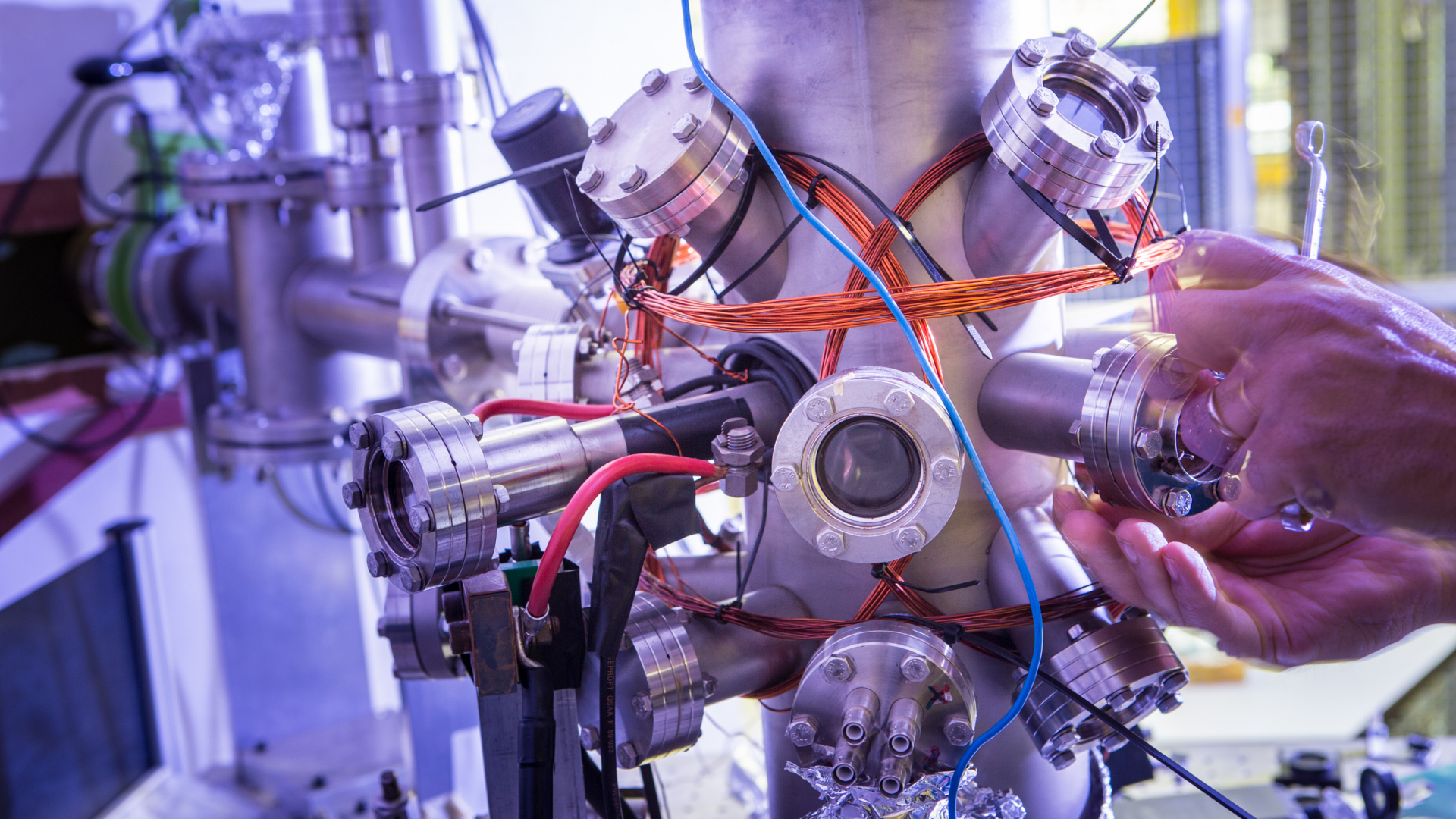
A special issue on plasma sources for advanced semiconductors responds to this mission, given that plasma sources are essential tools for manufacturing semiconductors. Laser-produced plasma (LPP) powers state-of-the-art nanolithography by generating the required extreme ultraviolet (EUV) light. Reducing the size of features in modern semiconductors is a major theme for semiconductor manufacturing where feature sizes are approaching nanometers, often as a part of complex, three-dimensional (3D) structures. Predicting, modeling, and measuring the properties of plasma from advanced sources with high resolution is at the forefront of research for many advanced industrial applications.
This Joint Special Topic Collection in Applied Physics Letters and Physics of Plasmas covers all of these areas, welcoming submissions reporting recent research results and perspectives in the field of plasma sources and their many important applications to semiconductor and relevant computational technologies developed to model these plasma sources. This collection includes 24 articles published in Applied Physics Letters3 and 13 articles in Physics of Plasmas.4 The combined 37 papers cover topics related to Plasma Sources for Advanced Semiconductor Applications, including modeling and experimental studies related to the generation of EUV light (and beyond) via LPP. It also includes papers devoted to experimental and modeling studies of plasma sources for plasma processing, and plasma etching and deposition.


