Universal warning signal for optical damage onset
Universal and easy-to-measure warning signals for catastrophic damage occur in the metals used to transport data in computer chips. That is what ARCNL PhD student Ester Abram discovered and described in a recent paper in the Journal of Applied Physics. “A slight increase in the observed reflectivity of the metal indicates that its morphology is starting to change as a result of exposure to laser light.”
While producing computer chips, silicon wafers are fed into a lithography machine. This machine illuminates patterns that are coated with thin film materials that ultimately become electronic circuits. After each illumination step, the wafer leaves the machine to be processed and then comes back for a next round of lines to be patterned. In order to precisely position these lines on top of each other, intense laser pulses are used to locate a set of position markers on the wafer.
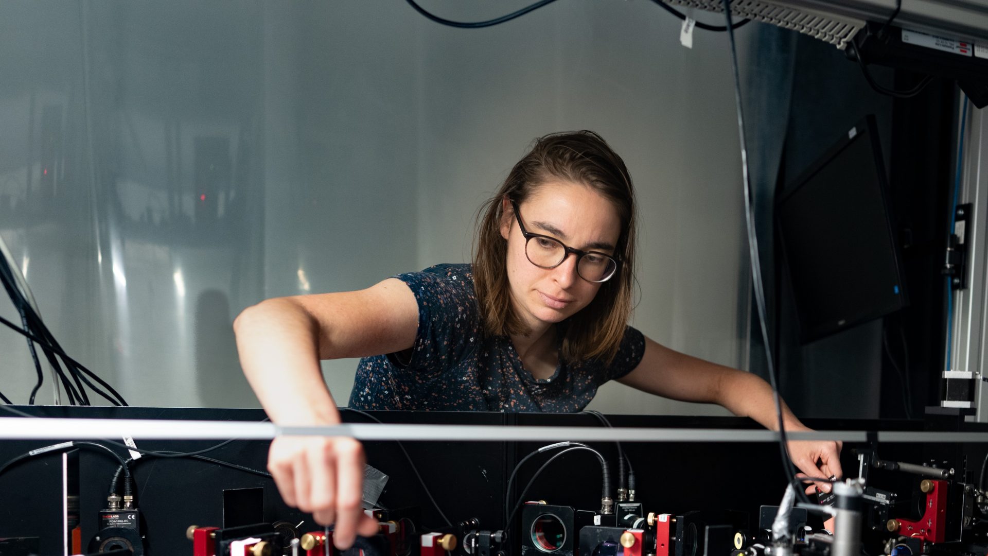
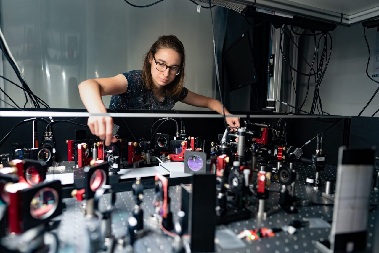
During this alignment step, the thin metallic layers are also exposed to this light, which might lead to damage. In the Light-Matter Interaction group of Paul Planken, Ester Abram studied these damage processes in nanometer-thick films of materials in a High Tech Systems and Materials (HTSM) research project.
Promising metal candidate
In her recent paper, Abram focusses on ruthenium as the metal of choice. Though ruthenium is not yet widely used in semiconductors, the metal is regarded as an interesting candidate to ultimately replace currently used materials like copper, which become less conductive as the electronic circuits shrink in size.
“We started our investigations with gold nanofilms as a model metal. Then we moved on to aluminum, to end up with ruthenium,” Abram explains. “We worked with grids consisting of 36 locations, which we each hit with an ultrashort, femtosecond laser pulse, increasing in intensity at each successive location. Then, we analyzed the metal layers with a myriad of microscopy techniques, ranging from Scanning Electron and Atomic Force Microscopy to Electron Backscatter Diffraction.”
Morphological changes
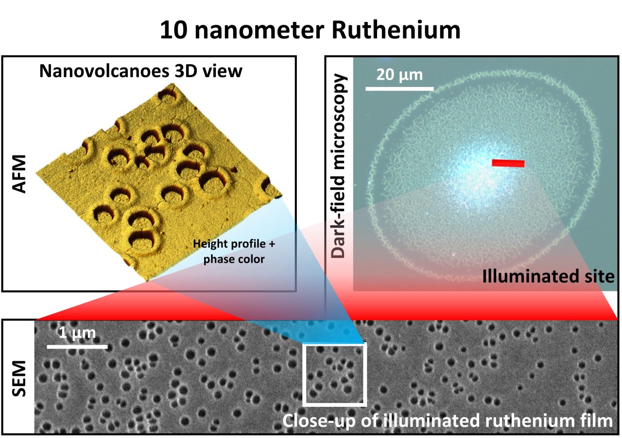
The PhD student found that, going from the lowest to the highest intensities, several regimes could be discerned in the morphology of the metal layers. At the lowest intensities, the metal withstands the laser pulses unaltered. From a certain intensity threshold on, small cracks start to appear. When the intensity of the laser pulse is increased even further, small features that the researchers dubbed nanovolcanoes start to form. And eventually, the ruthenium leaves the underlying substrate entirely.
However, before the cracks appear, the metal starts to deform, leaving a distinct fingerprint that can be used as an early warning signal, Abram discovered. “We studied the metal layers after exposure with a weak probe beam and measured their reflectivity. Early on, there is a small yet distinctive increase in the reflectivity of the metal, which in ruthenium can be up to 4 percent.”
Puzzling
Even though she found these types of optical changes rather early on during her PhD project in her experiments on aluminum, finding out what caused the reflectivity of the material to change took much longer, Abram explains. “Eventually, when my colleague Nikolai Orlov started using diffraction techniques on the ruthenium layers, we could resolve the grain size and that is when we found the root cause: beyond a certain threshold intensity level, the laser pulse results in localized melting, after which the ruthenium solidifies in larger grains than those found in the original material.”
Though in hindsight, it might sound rather straightforward that the light causes the ruthenium to melt, it is not self-evident at all, the researcher states. “The pulses are extremely short, resulting in ultrafast heating and cooling processes. It is rather remarkable that even in that short period of time, the material is able to reorientate.”
Practical use
The research result has a direct practical use: by monitoring reflectivity of the metal layer, one apparently can determine the maximum intensity the positioning laser is allowed to have to prevent damage to the conducting structures. This is highly relevant for the semiconductor industry.
Future plans
In the meantime, the researchers are building further on this result, Abram says. “We are looking at more complicated systems. While the study described in this paper looks at ruthenium on glass, we are now moving toward multilayer systems that better resemble the actual situation during chip production. And instead of flat metal surfaces, we also plan to look at gratings. Finally, the plan is to also study the effect of using multiple wavelengths and multiple pulses of laser light for the positioning of the wafer.”
Abram herself will not be involved in this specific research for much longer. “I have finished my thesis, which I will defend on June 20. So, besides working on two additional papers about my PhD project, I am now looking for a new opportunity to expand my professional experience in research or optics.”
Publication
Ester Abram, Nikolai Orlov, Erik C. Garnett, Paul Planken, Sub-ablation-threshold light-induced modification of thin ruthenium layers detected using optical reflectance, J. Appl. Phys. 136, 245305 (2024), https://doi.org/10.1063/5.0233239
Are you interested in Light-Matter interaction research? Then have a look at the Planken research group: https://arcnl.nl/research-groups/light-matter-interaction


